Ask us about
test equipment solutions for your industry
What is Electromagnetic Interference (EMI)?
Electromagnetic interference (EMI) is an undesired disturbance caused by electromagnetic radiation from an electronic device or system which negatively affects the performance of nearby electronic devices. EMI can manifest as electromagnetic emissions that disrupt the normal operation of sensitive electronic components and communication systems. In the context of EMC testing, EMI represents the assessment of a device’s impact as a source of unwanted RF emissions.
ATEC dives deep into the technical aspects of what EMI is, what causes it, and how to test for it. Read on below for more info.
What Causes Electromagnetic Interference?
EMI can be caused by many different things. A few examples include:
- Circuit Board Design: In general, EMC considerations need to be made throughout the whole research & design process. Something like long solder runs could create an unintentional emitting antenna.
- Switching Power Converters: Used in most circuitry as the power source, the switching frequency of the AC-DC or DC-DC inverter can create unintentional noise.
- Lack of EMI Shielding: PCBs (printed circuit boards) and electronic designs usually need some type of shielding to help achieve EMI compliance.
- Improper Grounding: This can also enhance EMI issues from the previous three points. For example, if your shielding is not properly grounded, you will not prevent EMI but in fact worsen it.
Natural phenomena such as lightning impulses, cranking the engine of a car, or the Internet of Things (IOT) world we are now living in can also cause EMI. Before testing was mandated, erroneous signals caused artillery to misfire and autopilot to veer off course. Our new reality is why the need for testing has become so important.
Types of Electromagnetic Interference
EMI is seen in two separate forms: radiated and conducted.
Radiated EMI originates from wireless communications in electronics, whereas conducted EMI is based upon power sources needed for the same devices. Though data and RF can be transmitted through a cable in many cases, EMI can occur as well (such as on a coaxial interconnecting cable or CAT6 cable).
Additional considerations for troubleshooting EMI issues in the radiated space is looking at the far field or near field EMF.
Near Field RF vs Far Field EMI
Understanding the mathematics and science behind an electromagnetic field, commonly referred to as EMF, can be complex when examining formulas. The diagram below best explains the structure of an RF wave in the far field, depicting both its electrical and magnetic field components. The key takeaway is to recognize that the near field and far field exhibit differences, and relying solely on the near field when measuring is not always sufficient.
Figure: Electromagnetic Wave Propagation of both E and H-Field.
Source: University Physics II – Thermodynamics, Electricity and Magnetism
Far field signals are crucial in full compliance testing and provide a more realistic characterization of a device’s emissions than the near field. On the other hand, near field RF is most useful in debugging circuits during the R&D process.
Figure: Near Field vs Far Field Wave Propagation from Source
Source: everything RF: What are Near Field and Far Field Regions of an Antenna?
For more information on EMF, read our blog: What is EMF & Why Is It Important?
Solving EMI Issues in PCBs
If equipped with using the proper test equipment, then pinpointing trouble spots within a PCB or other electronic devices can be easy.
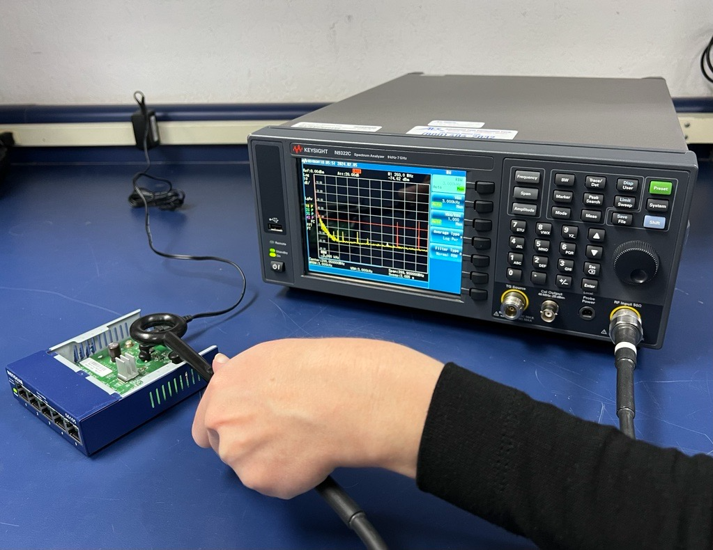
Basic EMI Test Setup
Using a spectrum analyzer, RF preamplifier, and near field probes will get you most of the way; with a few additional accessories needed for making an EMI measurement.

Image: Basic EMI test setup with DUT exceeding limits
Source: ATEC
Having near field measurements is a great place to start for pre-compliance emissions measurements. When developing a prototype device, being able to predict pass or fail results before further development will save time and money when it comes to full compliance testing.
How to Reduce Electromagnetic Interference (EMI)
EMI issues can occur in any type of electronic device, ranging from common items like a cell phone to sophisticated systems such as an avionic electrical system. Implementing certain measures can enhance the design process for any device, with emissions measurements serving as the initial step.
Reducing EMI starts at knowing what the causes are and being able to measure them. A few key factors to accomplishing this is:
- Proper grounding and shielding materials as needed.
- Use of EMI filters, decoupling capacitors, and ferrite chokes.
- PCB layout with minimal trace lengths.
Determining EMI and EMC issues may pose a challenge, but employing proper testing techniques can significantly simplify the process.
For questions about testing for EMI or what kinds of equipment you need, ATEC is happy to help out. Our wide inventory of EMC test equipment includes everything to complete either pre-compliance or full compliance, and our ATEC Assurance policy means risk-free renting. Reach out for a quote today.
